Login
Contact

Description
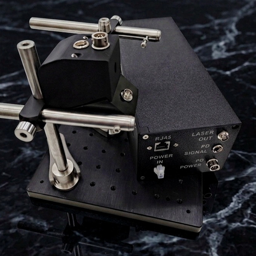
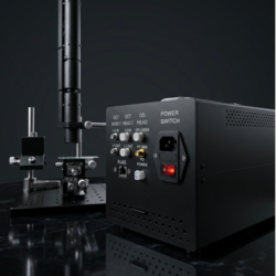
Optical Density (OD) scanning is a specialized technique used to measure ultra-thin films with thicknesses below 1 μm. It employs a highly stable optical measurement system to estimate a material’s absorption coefficient and absorption thickness. This method is non-contact and non-invasive, making it suitable for high-resolution imaging analysis.
OD optical density scanning is one of the few techniques capable of achieving nanometer-level resolution in thin film thickness measurement. It is particularly well-suited for applications in semiconductor thin-film processing, precision optical coatings, and quality inspection and process control of ultra-thin photoresists. As such, it is considered one of the key technologies in modern precision metrology.
OD optical density scanning is one of the few techniques capable of achieving nanometer-level resolution in thin film thickness measurement. It is particularly well-suited for applications in semiconductor thin-film processing, precision optical coatings, and quality inspection and process control of ultra-thin photoresists. As such, it is considered one of the key technologies in modern precision metrology.
Related Products
Optical Coherence Tomography
You may also like
Highest Rated Products
Back
 Product Inquiry